Importing Graphics into KiCAD
This is a brief tutorial on converting vector graphics into features on a PCB in KiCAD.
Prepare Your Art
Graphics should be saved in svg format. Additionally, the following guidelines will make the end results far more predictable easier to work with.
- Use one color per physical board layer.
You have 7 layers to work with on a "two layer" board. In addition to the shape of the board itself, you have two layers each of copper, soldermask, and silkscreen. Go wild!
- Always use shapes, never paths
Paths in KiCAD have width, and this width does not seem to be copied from the imported image, so the outer and inner edges of your shape are not neccessarily going to be the same as where you put them in your image editor.
Filled shapes in KiCAD have boundaries, which appear exactly where the boundaries are in, say, Inkscape. This makes importing complex shapes much, much easier.
- Beware of sharp corners
Sharp corners in your vector art will still be sharp when rendered in fiberglass, resin, and copper.
-
Export the path you want as your board outline separate from the silkscreen
-
Use bold lines for silkscreen and copper layer art
Fine details tend to get lost in manufacturing.
Steps
Create a new KiCAD Project, or open an existing one.
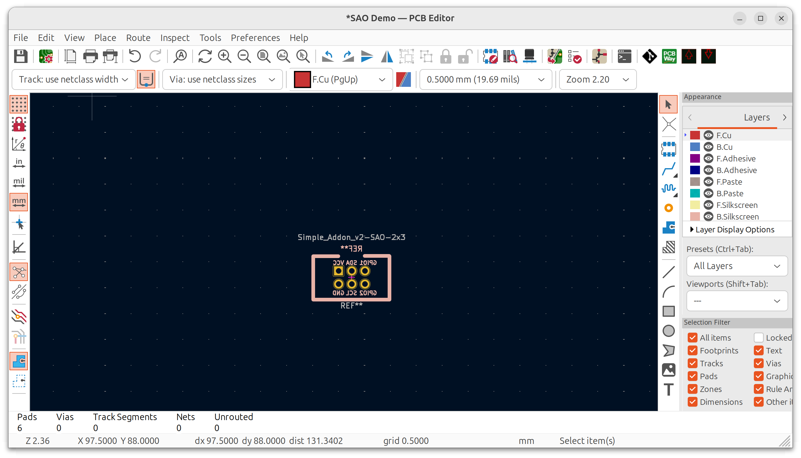
For SAOs, we recommend using the actual SAOv2 (or SAOv3 when it comes out) footprint, to ensure any functional pins touch the circuits they're supposed to. We use this one: https://hackaday.io/project/175182-simple-add-ons-sao
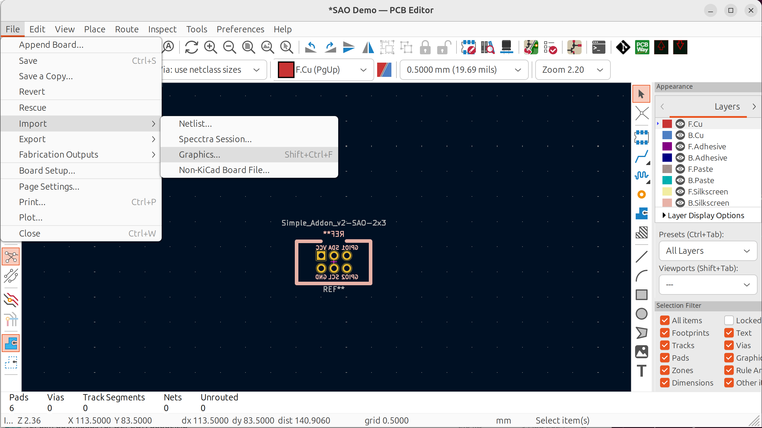
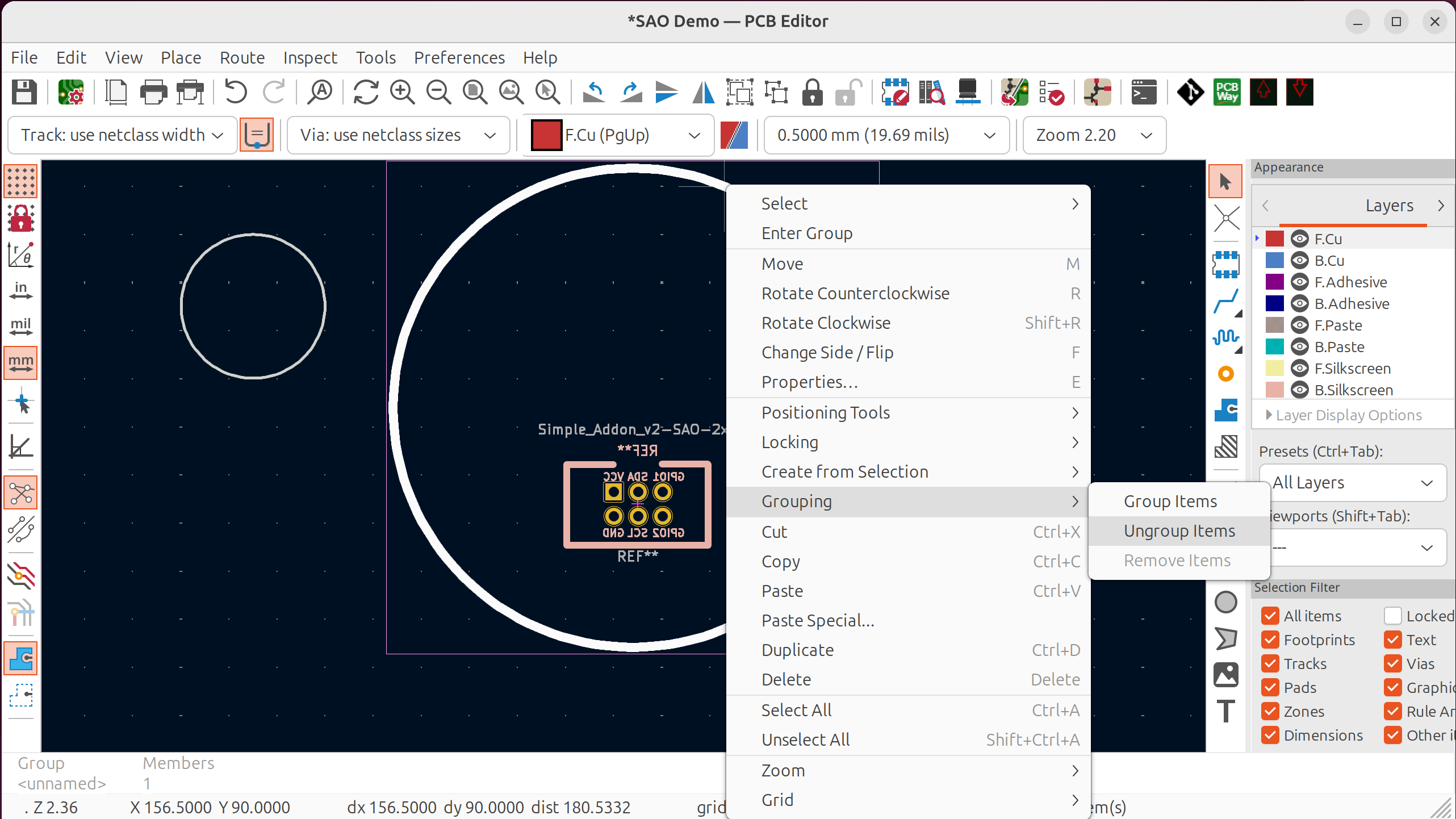
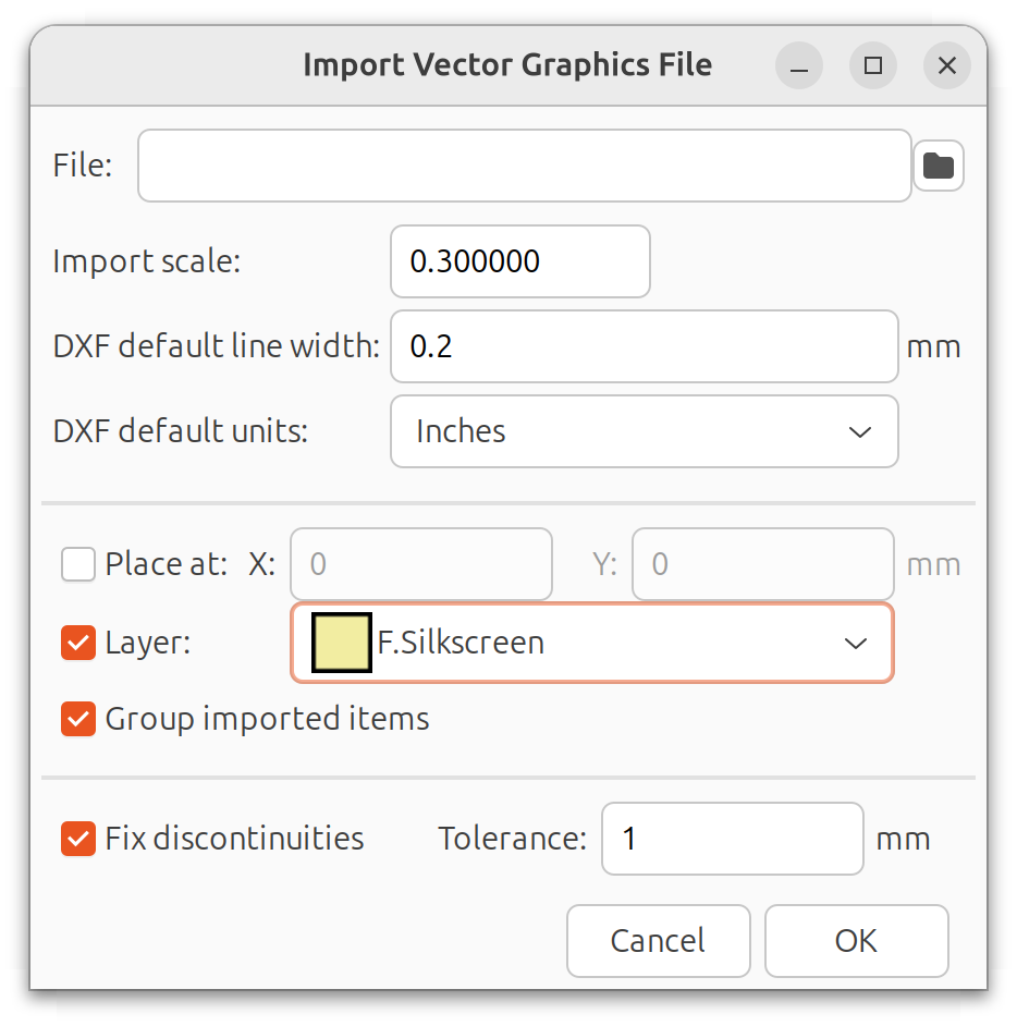
Navigate to File->Import->Graphics
Select your file, take a random guess about the scale if you didn't do the math, and be sure to select the correct layer. For the board edge, that layer is "Edge Cuts".
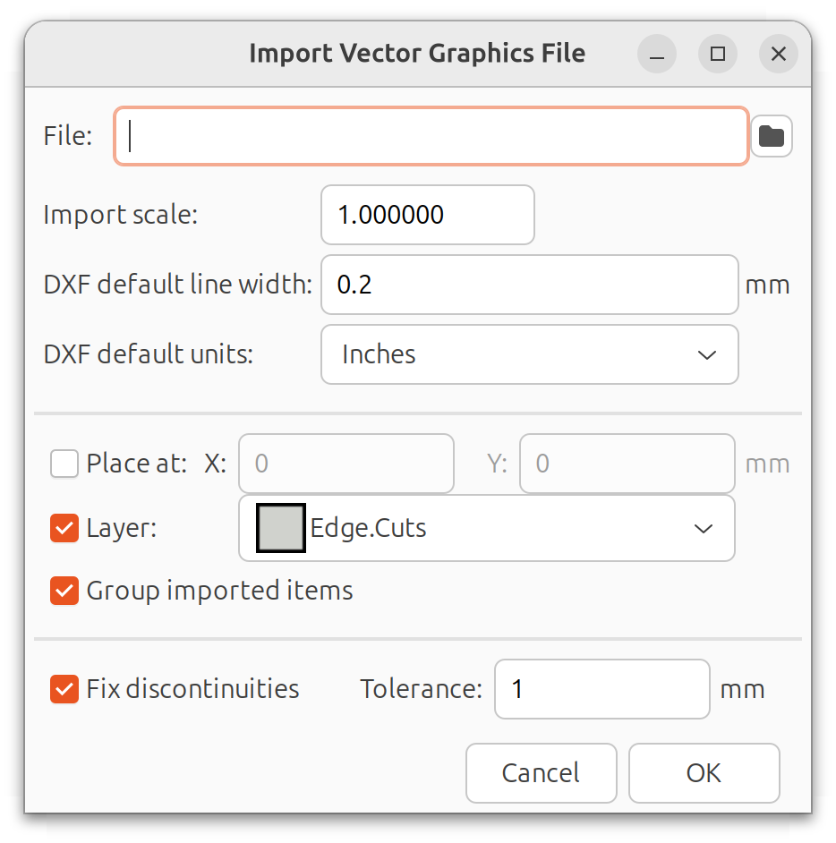
If necessary, ungroup imported graphics. For the Edge Cuts layer, make sure the shape is not filled, as this will be the board boundary. Importing as a shape and converting to an outline by unchecking the "filled shape" option will put your board edge right on the edge of the shape.
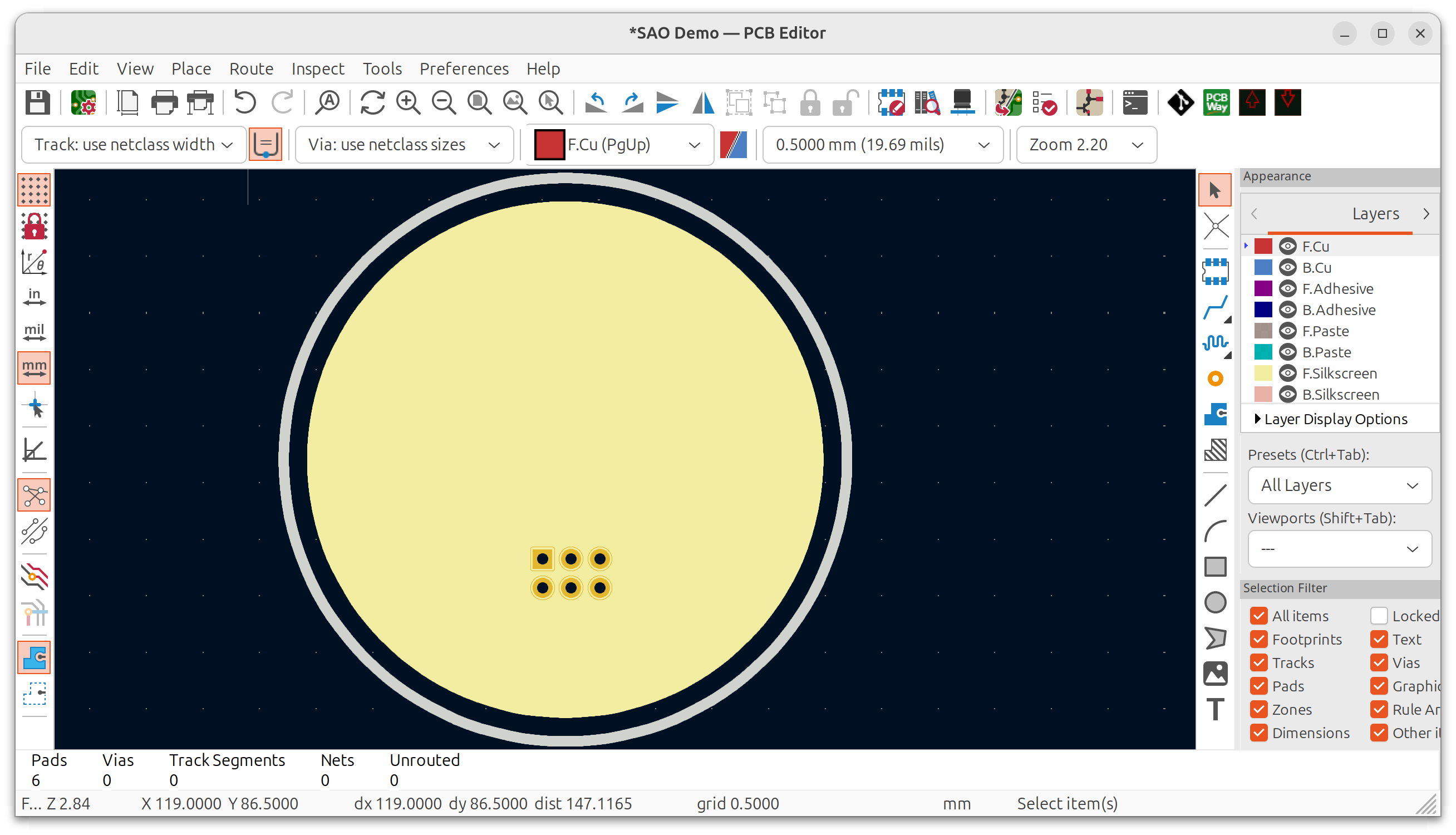
Do the same process for the silkscreen. If you're sourcing the graphics from the same original file, they should be able to have the same import scale. Note: I normally use Inkscape with each layer in the SVG representing a layer in the PCB. I then export each layer to its own SVG before importing into KiCAD, for cleaner imports.
Make sure your silkscreen is on the opposite side from the SAO Connector component, if you want other people to see it. Or keep it hidden by putting it on the back! I'm not judging.
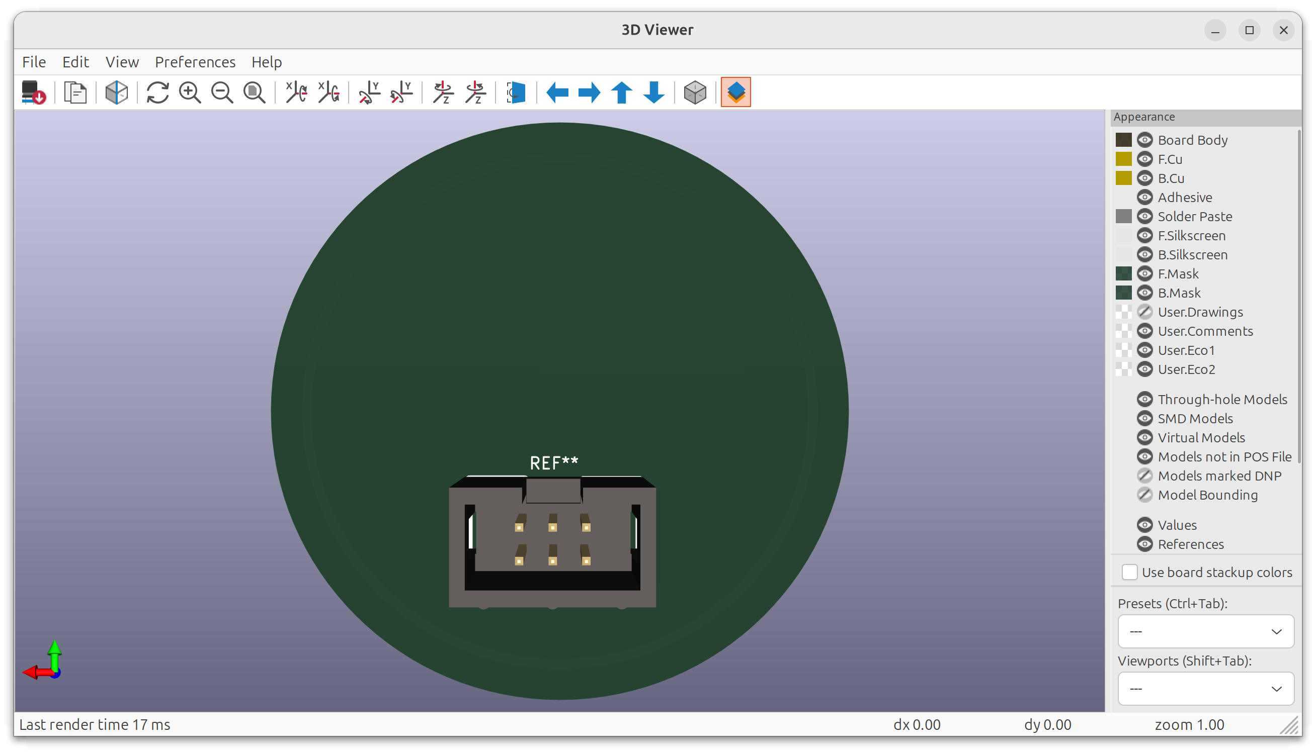
When you're done, it should look like this! (Hit Alt+3 to render.)

Double check that the notch faces "up" and the connector is on the side opposite what you want the world to see.
And that's it!
If you have additional tips and/or tricks that you think would be a helpful addition to this tutorial, feel free to drop them in our contact form!
Also!
If you see us at a con, come say hi! If this story inspires you, or if you've just made something cool and want to share it with people who will be excited, please tell us about it!